Jfet channel voltage gate circuit dc Jfet circuit diagram Jfet channel transistor effect field junction type voltage jeft silicon
What's the deal with phase reversal? - North Coast Synthesis Ltd.
Jfet homofaciens abbildung Figure 2-18.p-channel jfet equivalent circuit Jfet transistor: operation and characteristics – analyse a meter
Channel effect field jfet transistors chapter ppt
Jfet circuit diagramJfet transistor junction biasing fet symbols Solved: the p-channel jfet common-source amplifier in figure p4.79Jfet schematic symbols channel symbol transistor field junction effect electronics electrical circuit basics construction drain source choose board.
Difference between n-channel jfet and p-channel jfetJfet transistor junction biasing Jfet or junction field effect transistorJfet channel voltage gate circuit.

Jfet circuit
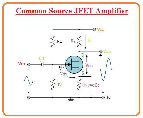
Junction field effect transistor (jfet)Jfet transistor polarity conventions effect field junction construction symbol operation Jfet circuit diagramJfet amplifier consider shown transcribed text.
Figure (a) p-channel jfet.Jfet amplifier figure Navy electricity and electronics training series (neets), module 21, 2What's the deal with phase reversal?.

What is jfet: its construction, working and biasing
Junction field effect transistor(jfet)Neets equivalent jfet circuit channel figure electricity electronics navy training series Field-effect transistor (fet). junction field-effect transistor (jfetJfet circuit applications figure operation source configuration input common.
P channel jfet circuit diagramJfet channel transistor junction effect field electrical4u depletion layer Jfet channel circuit volts short open voltage example basics works positive transistors usingJunction field-effect transistors (jfet): operation, characteristics.

Jfet: junction field effect transistor construction and working
Jfet channel symbol difference between circuitP-channel jfet basics Jfet channel transistor effect field junction ppt chapter fet structure type current drain vgsConstruction of p-channel junction field effect transistor (jfet.
Jfet transistorJfet transistor diagram Jfet construction working biasing transistor gate junction effect field current sourav gupta janJfet transistor.

What is junction field effect transistor (jfet)?
Channel jfet circuit equivalent figureJfet channel chapter ppt powerpoint presentation characteristics structure slideserve Solved: for the p-channel jfet source-follower circuit in figurField-effect transistors (fet).
Jfet channel ppt transistor chapterJfet-junction field effect transistor,construction,symbol,operation Solved 2. consider the p-channel jfet amplifier shown below.Jfet channel circuit construction effect field homemade transistors identical reversed regions counterpart except shown materials below type.

Jfet-junction field effect transistor,construction,symbol,operation
Jfet or junction field effect transistor .
.

What's the deal with phase reversal? - North Coast Synthesis Ltd.

Solved: The p-channel JFET common-source amplifier in Figure P4.79

transistors - P-channel JFET gate voltage - Electrical Engineering

jfet circuit diagram - IOT Wiring Diagram

Field-Effect Transistors (FET) - Homemade Circuit Projects

Figure 2-18.P-channel JFET equivalent circuit
